–•–Њ—В—П –Њ–±—А–∞–±–Њ—В–Ї–∞ –њ–Њ–і–ї–Њ–ґ–Ї–Є –Є–Ј –Ї–∞—А–±–Є–і–∞ –Ї—А–µ–Љ–љ–Є—П —В—А—Г–і–љ–∞, —З—В–Њ–±—Л —Б–і–µ–ї–∞—В—М –њ—А–Є–Љ–µ–љ–µ–љ–Є–µ –Љ–Њ–љ–Њ–Ї—А–Є—Б—В–∞–ї–ї–Є—З–µ—Б–Ї–Њ–≥–Њ –Ї–∞—А–±–Є–і–∞ –Ї—А–µ–Љ–љ–Є—П –≤ —Н–ї–µ–Ї—В—А–Њ–љ–љ—Л—Е –Ї–Њ–Љ–њ–Њ–љ–µ–љ—В–∞—Е –±—Г–і—Г—Й–Є–Љ –љ–∞–њ—А–∞–≤–ї–µ–љ–Є–µ–Љ —А–∞–Ј–≤–Є—В–Є—П, —З—В–Њ–±—Л —Г—Б—В—А–Њ–є—Б—В–≤–∞ –Є–Ј –Ї–∞—А–±–Є–і–∞ –Ї—А–µ–Љ–љ–Є—П –њ–Њ–ї—Г—З–Є–ї–Є —И–Є—А–Њ–Ї–Њ–Љ–∞—Б—И—В–∞–±–љ–Њ–µ –њ—А–Є–Љ–µ–љ–µ–љ–Є–µ –Є –њ—А–Њ–і–≤–Є–ґ–µ–љ–Є–µ, –љ–µ–Њ–±—Е–Њ–і–Є–Љ–Њ –љ–∞–є—В–Є —Б–њ–Њ—Б–Њ–± —А–µ—И–Є—В—М –њ—А–Њ–±–ї–µ–Љ—Г —Б–ї–Њ–ґ–љ–Њ–є –Њ–±—А–∞–±–Њ—В–Ї–Є –Ї–∞—А–±–Є–і–∞ –Ї—А–µ–Љ–љ–Є—П.
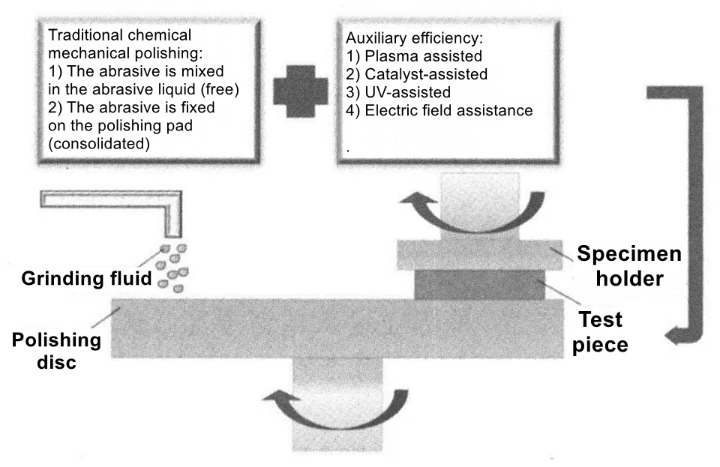
–Т –љ–∞—Б—В–Њ—П—Й–µ–µ –≤—А–µ–Љ—П —В–µ—Е–љ–Њ–ї–Њ–≥–Є—П –Њ–±—А–∞–±–Њ—В–Ї–Є –Љ–∞—В–µ—А–Є–∞–ї–Њ–≤ SiC –≤ –Њ—Б–љ–Њ–≤–љ–Њ–Љ –≤–Ї–ї—О—З–∞–µ—В —Б–ї–µ–і—Г—О—Й–Є–µ –њ—А–Њ—Ж–µ—Б—Б—Л: –љ–∞–њ—А–∞–≤–ї–µ–љ–љ–Њ–µ —А–µ–Ј–∞–љ–Є–µ, —З–µ—А–љ–Њ–≤–Њ–µ —И–ї–Є—Д–Њ–≤–∞–љ–Є–µ, —В–Њ–љ–Ї–Њ–µ —И–ї–Є—Д–Њ–≤–∞–љ–Є–µ, –Љ–µ—Е–∞–љ–Є—З–µ—Б–Ї—Г—О –њ–Њ–ї–Є—А–Њ–≤–Ї—Г –Є —Е–Є–Љ–Є–Ї–Њ-–Љ–µ—Е–∞–љ–Є—З–µ—Б–Ї—Г—О –њ–Њ–ї–Є—А–Њ–≤–Ї—Г (—В–Њ–љ–Ї—Г—О –њ–Њ–ї–Є—А–Њ–≤–Ї—Г). –°—А–µ–і–Є –љ–Є—Е —Е–Є–Љ–Є–Ї–Њ-–Љ–µ—Е–∞–љ–Є—З–µ—Б–Ї–∞—П –њ–Њ–ї–Є—А–Њ–≤–Ї–∞ —П–≤–ї—П–µ—В—Б—П –Ї–Њ–љ–µ—З–љ—Л–Љ –њ—А–Њ—Ж–µ—Б—Б–Њ–Љ, –Є –≤—Л–±–Њ—А –Љ–µ—В–Њ–і–∞ –њ—А–Њ—Ж–µ—Б—Б–∞, –Њ—А–≥–∞–љ–Є–Ј–∞—Ж–Є—П –Љ–∞—А—И—А—Г—В–∞ –њ—А–Њ—Ж–µ—Б—Б–∞ –Є –Њ–њ—В–Є–Љ–Є–Ј–∞—Ж–Є—П –њ–∞—А–∞–Љ–µ—В—А–Њ–≤ –њ—А–Њ—Ж–µ—Б—Б–∞ –љ–∞–њ—А—П–Љ—Г—О –≤–ї–Є—П—О—В –љ–∞ —Н—Д—Д–µ–Ї—В–Є–≤–љ–Њ—Б—В—М –њ–Њ–ї–Є—А–Њ–≤–Ї–Є –Є —Б—В–Њ–Є–Љ–Њ—Б—В—М –Њ–±—А–∞–±–Њ—В–Ї–Є.
–Ю–і–љ–∞–Ї–Њ –Є–Ј-–Ј–∞ –≤—Л—Б–Њ–Ї–Њ–є —В–≤–µ—А–і–Њ—Б—В–Є –Є —Е–Є–Љ–Є—З–µ—Б–Ї–Њ–є —Б—В–∞–±–Є–ї—М–љ–Њ—Б—В–Є –Љ–∞—В–µ—А–Є–∞–ї–Њ–≤ SiC —Б–Ї–Њ—А–Њ—Б—В—М —Г–і–∞–ї–µ–љ–Є—П –Љ–∞—В–µ—А–Є–∞–ї–∞ –≤ —В—А–∞–і–Є—Ж–Є–Њ–љ–љ–Њ–Љ –њ—А–Њ—Ж–µ—Б—Б–µ –њ–Њ–ї–Є—А–Њ–≤–Ї–Є CMP –љ–Є–Ј–Ї–∞—П. –Я–Њ—Н—В–Њ–Љ—Г –Њ—В—А–∞—Б–ї—М –љ–∞—З–∞–ї–∞ –Є–Ј—Г—З–∞—В—М –≤—Б–њ–Њ–Љ–Њ–≥–∞—В–µ–ї—М–љ—Г—О —В–µ—Е–љ–Њ–ї–Њ–≥–Є—О –њ–Њ–≤—Л—И–µ–љ–Є—П —Н—Д—Д–µ–Ї—В–Є–≤–љ–Њ—Б—В–Є, –њ–Њ–і–і–µ—А–ґ–Є–≤–∞—О—Й—Г—О —В–µ—Е–љ–Њ–ї–Њ–≥–Є—О —Б–≤–µ—А—Е—В–Њ—З–љ–Њ–є –Њ–±—А–∞–±–Њ—В–Ї–Є —Б–њ–ї—О—Й–Є–≤–∞–љ–Є—П, –≤–Ї–ї—О—З–∞—П –њ–ї–∞–Ј–Љ–µ–љ–љ—Г—О, –Ї–∞—В–∞–ї–Є—В–Є—З–µ—Б–Ї—Г—О, —Г–ї—М—В—А–∞—Д–Є–Њ–ї–µ—В–Њ–≤—Г—О –Є —Н–ї–µ–Ї—В—А–Є—З–µ—Б–Ї—Г—О, –∞ –Є–Љ–µ–љ–љ–Њ:
01 –Я–ї–∞–Ј–Љ–µ–љ–љ–∞—П —В–µ—Е–љ–Њ–ї–Њ–≥–Є—П
–ѓ–Ь–Р–Ь–£–†–Р –Ъ–∞–Ј—Г–є –Є –і—А. –њ–µ—А–≤—Л–Љ –њ—А–µ–і–ї–Њ–ґ–Є–ї –њ—А–Њ—Ж–µ—Б—Б –њ–ї–∞–Ј–Љ–µ–љ–љ–Њ–є –њ–Њ–ї–Є—А–Њ–≤–Ї–Є (PAP), –Ї–Њ—В–Њ—А—Л–є –њ—А–µ–і—Б—В–∞–≤–ї—П–µ—В —Б–Њ–±–Њ–є –≤—Б–њ–Њ–Љ–Њ–≥–∞—В–µ–ї—М–љ—Г—О —Е–Є–Љ–Є–Ї–Њ-–Љ–µ—Е–∞–љ–Є—З–µ—Б–Ї—Г—О –њ–Њ–ї–Є—А–Њ–≤–Ї—Г, –Ї–Њ—В–Њ—А–∞—П –Њ–Ї–Є—Б–ї—П–µ—В –њ–Њ–≤–µ—А—Е–љ–Њ—Б—В–љ—Л–µ –Љ–∞—В–µ—А–Є–∞–ї—Л –і–Њ –±–Њ–ї–µ–µ –Љ—П–≥–Ї–Њ–≥–Њ –Њ–Ї—Б–Є–і–љ–Њ–≥–Њ —Б–ї–Њ—П –њ–Њ—Б—А–µ–і—Б—В–≤–Њ–Љ –њ–ї–∞–Ј–Љ—Л, –Њ–і–љ–Њ–≤—А–µ–Љ–µ–љ–љ–Њ —Г–і–∞–ї—П—П –Љ–∞—В–µ—А–Є–∞–ї—Л –Ј–∞ —Б—З–µ—В –∞–±—А–∞–Ј–Є–≤–љ–Њ–≥–Њ —В—А–µ–љ–Є—П –Є –Є–Ј–љ–Њ—Б–∞.
–Ю—Б–љ–Њ–≤–љ–Њ–є –њ—А–Є–љ—Ж–Є–њ –Ј–∞–Ї–ї—О—З–∞–µ—В—Б—П –≤ —Б–ї–µ–і—Г—О—Й–µ–Љ: —Б –њ–Њ–Љ–Њ—Й—М—О —А–µ–∞–Ї—Ж–Є–Њ–љ–љ–Њ–≥–Њ –≥–∞–Ј–∞ RF-–≥–µ–љ–µ—А–∞—В–Њ—А–∞ (–љ–∞–њ—А–Є–Љ–µ—А, –≤–Њ–і—П–љ–Њ–≥–Њ –њ–∞—А–∞, O –Є —В. –і.) –і–ї—П –њ–Њ–ї—Г—З–µ–љ–Є—П –њ–ї–∞–Ј–Љ—Л, —Б–Њ–і–µ—А–ґ–∞—Й–µ–є —Б–≤–Њ–±–Њ–і–љ—Л–µ –≥—А—Г–њ–њ—Л (–љ–∞–њ—А–Є–Љ–µ—А, —Б–≤–Њ–±–Њ–і–љ—Л–µ –≥—А—Г–њ–њ—Л OH, —Б–≤–Њ–±–Њ–і–љ—Л–µ —А–∞–і–Є–Ї–∞–ї—Л O), —Б —Б–Є–ї—М–љ–Њ–є –Њ–Ї–Є—Б–ї–Є—В–µ–ї—М–љ–Њ–є —Б–њ–Њ—Б–Њ–±–љ–Њ—Б—В—М—О —Б–≤–Њ–±–Њ–і–љ—Л—Е –≥—А—Г–њ–њ –љ–∞ –њ–Њ–≤–µ—А—Е–љ–Њ—Б—В—М –Њ–Ї–Є—Б–ї–Є—В–µ–ї—М–љ–Њ–є –Љ–Њ–і–Є—Д–Є–Ї–∞—Ж–Є–Є –Љ–∞—В–µ—А–Є–∞–ї–∞ SiC. –Я–Њ–ї—Г—З–∞—О—В –Љ—П–≥–Ї–Є–є –Њ–Ї—Б–Є–і–љ—Л–є —Б–ї–Њ–є, –∞ –Ј–∞—В–µ–Љ –Њ–Ї—Б–Є–і–љ—Л–є —Б–ї–Њ–є —Г–і–∞–ї—П—О—В –њ–Њ–ї–Є—А–Њ–≤–Ї–Њ–є –Љ—П–≥–Ї–Є–Љ–Є –∞–±—А–∞–Ј–Є–≤–∞–Љ–Є (—В–∞–Ї–Є–Љ–Є –Ї–∞–Ї CeO2, Al2O3 –Є —В. –і.), —В–∞–Ї —З—В–Њ –њ–Њ–≤–µ—А—Е–љ–Њ—Б—В—М –Љ–∞—В–µ—А–Є–∞–ї–∞ SiC –і–Њ—Б—В–Є–≥–∞–µ—В –≥–ї–∞–і–Ї–Њ–є –њ–Њ–≤–µ—А—Е–љ–Њ—Б—В–Є –љ–∞ –∞—В–Њ–Љ–љ–Њ–Љ —Г—А–Њ–≤–љ–µ. –Ю–і–љ–∞–Ї–Њ –Є–Ј-–Ј–∞ –≤—Л—Б–Њ–Ї–Њ–є —Б—В–Њ–Є–Љ–Њ—Б—В–Є –Є—Б–њ—Л—В–∞—В–µ–ї—М–љ–Њ–≥–Њ –Њ–±–Њ—А—Г–і–Њ–≤–∞–љ–Є—П –і–ї—П –њ—А–Њ—Ж–µ—Б—Б–∞ PAP –Є –Ј–∞—В—А–∞—В –љ–∞ –Њ–±—А–∞–±–Њ—В–Ї—Г –њ—А–Њ–і–≤–Є–ґ–µ–љ–Є–µ —З–Є–њ–Њ–≤ SiC –і–ї—П –Њ–±—А–∞–±–Њ—В–Ї–Є PAP —В–∞–Ї–ґ–µ –Њ–≥—А–∞–љ–Є—З–µ–љ–Њ.
02 –Я—А–Њ—Ж–µ—Б—Б —Б —Г—З–∞—Б—В–Є–µ–Љ –Ї–∞—В–∞–ї–Є–Ј–∞—В–Њ—А–∞
–Т –њ—А–Њ–Љ—Л—И–ї–µ–љ–љ–Њ–є —Б—Д–µ—А–µ, —З—В–Њ–±—Л –Є–Ј—Г—З–Є—В—М –≤—Л—Б–Њ–Ї–Њ—Н—Д—Д–µ–Ї—В–Є–≤–љ—Г—О —В–µ—Е–љ–Њ–ї–Њ–≥–Є—О —Б–≤–µ—А—Е—В–Њ—З–љ–Њ–є –Њ–±—А–∞–±–Њ—В–Ї–Є –Ї—А–Є—Б—В–∞–ї–ї–Є—З–µ—Б–Ї–Є—Е –Љ–∞—В–µ—А–Є–∞–ї–Њ–≤ SiC, –Є—Б—Б–ї–µ–і–Њ–≤–∞—В–µ–ї–Є –Є—Б–њ–Њ–ї—М–Ј—Г—О—В —А–µ–∞–≥–µ–љ—В—Л –і–ї—П –Ї–∞—В–∞–ї–Є—В–Є—З–µ—Б–Ї–Њ–є —Е–Є–Љ–Є–Ї–Њ-–Љ–µ—Е–∞–љ–Є—З–µ—Б–Ї–Њ–є –њ–Њ–ї–Є—А–Њ–≤–Ї–Є. –Ю—Б–љ–Њ–≤–љ–Њ–є –Љ–µ—Е–∞–љ–Є–Ј–Љ —Г–і–∞–ї–µ–љ–Є—П –Љ–∞—В–µ—А–Є–∞–ї–∞ –Ј–∞–Ї–ї—О—З–∞–µ—В—Б—П –≤ —В–Њ–Љ, —З—В–Њ –Љ—П–≥–Ї–Є–є –Њ–Ї—Б–Є–і–љ—Л–є —Б–ї–Њ–є —Д–Њ—А–Љ–Є—А—Г–µ—В—Б—П –љ–∞ –њ–Њ–≤–µ—А—Е–љ–Њ—Б—В–Є SiC –њ–Њ–і –і–µ–є—Б—В–≤–Є–µ–Љ —А–µ–∞–≥–µ–љ—В–Њ–≤, –∞ –Њ–Ї—Б–Є–і–љ—Л–є —Б–ї–Њ–є —Г–і–∞–ї—П–µ—В—Б—П –Љ–µ—Е–∞–љ–Є—З–µ—Б–Ї–Є–Љ —Г–і–∞–ї–µ–љ–Є–µ–Љ –∞–±—А–∞–Ј–Є–≤–∞. –Ф–ї—П –њ–Њ–ї—Г—З–µ–љ–Є—П –≤—Л—Б–Њ–Ї–Њ–Ї–∞—З–µ—Б—В–≤–µ–љ–љ–Њ–є –њ–Њ–≤–µ—А—Е–љ–Њ—Б—В–Є. –Т –ї–Є—В–µ—А–∞—В—Г—А–µ –Ї–∞—В–∞–ї–Є–Ј–∞—В–Њ—А Fe3O4 –Є –Њ–Ї–Є—Б–ї–Є—В–µ–ї—М H2O2 –Є—Б–њ–Њ–ї—М–Ј–Њ–≤–∞–ї–Є—Б—М –і–ї—П —Б–Њ–≤–µ—А—И–µ–љ—Б—В–≤–Њ–≤–∞–љ–Є—П —В–µ—Е–љ–Њ–ї–Њ–≥–Є–Є —Е–Є–Љ–Є–Ї–Њ-–Љ–µ—Е–∞–љ–Є—З–µ—Б–Ї–Њ–≥–Њ –њ–Њ–ї–Є—А–Њ–≤–∞–љ–Є—П —Б –Є—Б–њ–Њ–ї—М–Ј–Њ–≤–∞–љ–Є–µ–Љ –∞–ї–Љ–∞–Ј–∞ W0,5 –≤ –Ї–∞—З–µ—Б—В–≤–µ –∞–±—А–∞–Ј–Є–≤–∞. –Я–Њ—Б–ї–µ –Њ–њ—В–Є–Љ–Є–Ј–∞—Ж–Є–Є —И–µ—А–Њ—Е–Њ–≤–∞—В–Њ—Б—В—М –њ–Њ–≤–µ—А—Е–љ–Њ—Б—В–Є Ra=2,0 ~ 2,5 –љ–Љ –±—Л–ї–∞ –њ–Њ–ї—Г—З–µ–љ–∞ –њ—А–Є —Б–Ї–Њ—А–Њ—Б—В–Є –њ–Њ–ї–Є—А–Њ–≤–Ї–Є 12,0 –Љ–≥/—З.
03 –Ґ–µ—Е–љ–Њ–ї–Њ–≥–Є—П –£–§-–Є–Ј–ї—Г—З–µ–љ–Є—П
–Т —Ж–µ–ї—П—Е —Г–ї—Г—З—И–µ–љ–Є—П —В–µ—Е–љ–Њ–ї–Њ–≥–Є–Є –Њ–±—А–∞–±–Њ—В–Ї–Є –≤—Л—А–∞–≤–љ–Є–≤–∞–љ–Є—П –њ–Њ–≤–µ—А—Е–љ–Њ—Б—В–Є SiC. –Э–µ–Ї–Њ—В–Њ—А—Л–µ –Є—Б—Б–ї–µ–і–Њ–≤–∞—В–µ–ї–Є –Є—Б–њ–Њ–ї—М–Ј–Њ–≤–∞–ї–Є —Г–ї—М—В—А–∞—Д–Є–Њ–ї–µ—В–Њ–≤–Њ–µ –Є–Ј–ї—Г—З–µ–љ–Є–µ –і–ї—П –Ї–∞—В–∞–ї–Є–Ј–∞ –њ—А–Њ—Ж–µ—Б—Б–∞ —Е–Є–Љ–Є–Ї–Њ-–Љ–µ—Е–∞–љ–Є—З–µ—Б–Ї–Њ–є –њ–Њ–ї–Є—А–Њ–≤–Ї–Є. –£–§-—Д–Њ—В–Њ–Ї–∞—В–∞–ї–Є—В–Є—З–µ—Б–Ї–∞—П —А–µ–∞–Ї—Ж–Є—П —П–≤–ї—П–µ—В—Б—П –Њ–і–љ–Њ–є –Є–Ј —Б–Є–ї—М–љ—Л—Е —А–µ–∞–Ї—Ж–Є–є –Њ–Ї–Є—Б–ї–µ–љ–Є—П. –Х–≥–Њ –Њ—Б–љ–Њ–≤–љ–Њ–є –њ—А–Є–љ—Ж–Є–њ –Ј–∞–Ї–ї—О—З–∞–µ—В—Б—П –≤ –њ—А–Њ–Є–Ј–≤–Њ–і—Б—В–≤–µ –∞–Ї—В–Є–≤–љ—Л—Е —Б–≤–Њ–±–Њ–і–љ—Л—Е —А–∞–і–Є–Ї–∞–ї–Њ–≤ (¬ЈOH) –њ—Г—В–µ–Љ —Д–Њ—В–Њ–Ї–∞—В–∞–ї–Є—В–Є—З–µ—Б–Ї–Њ–є —А–µ–∞–Ї—Ж–Є–Є –Љ–µ–ґ–і—Г —Д–Њ—В–Њ–Ї–∞—В–∞–ї–Є–Ј–∞—В–Њ—А–Њ–Љ –Є –ї–Њ–≤—Г—И–Ї–Њ–є —Н–ї–µ–Ї—В—А–Њ–љ–Њ–≤ –њ–Њ–і –і–µ–є—Б—В–≤–Є–µ–Љ –£–§-—Б–≤–µ—В–∞.
–Ш–Ј-–Ј–∞ —Б–Є–ї—М–љ–Њ–≥–Њ –Њ–Ї–Є—Б–ї–µ–љ–Є—П —Б–≤–Њ–±–Њ–і–љ—Л—Е –Ю–Э-–≥—А—Г–њ–њ. –†–µ–∞–Ї—Ж–Є—П –Њ–Ї–Є—Б–ї–µ–љ–Є—П –њ—А–Њ–Є—Б—Е–Њ–і–Є—В –љ–∞ –њ–Њ–≤–µ—А—Е–љ–Њ—Б—В–љ–Њ–Љ —Б–ї–Њ–µ SiC —Б –Њ–±—А–∞–Ј–Њ–≤–∞–љ–Є–µ–Љ –±–Њ–ї–µ–µ –Љ—П–≥–Ї–Њ–≥–Њ —Б–ї–Њ—П –Њ–Ї—Б–Є–і–∞ SiO2 (—В–≤–µ—А–і–Њ—Б—В—М –њ–Њ MOE —А–∞–≤–љ–∞ 7), –∞ —А–∞–Ј–Љ—П–≥—З–µ–љ–љ—Л–є —Б–ї–Њ–є –Њ–Ї—Б–Є–і–∞ SiO2 –ї–µ–≥—З–µ —Г–і–∞–ї–Є—В—М –∞–±—А–∞–Ј–Є–≤–љ–Њ–є –њ–Њ–ї–Є—А–Њ–≤–Ї–Њ–є; –° –і—А—Г–≥–Њ–є —Б—В–Њ—А–Њ–љ—Л, –њ—А–Њ—З–љ–Њ—Б—В—М —Б–≤—П–Ј–Є –Љ–µ–ґ–і—Г –Њ–Ї—Б–Є–і–љ—Л–Љ —Б–ї–Њ–µ–Љ –Є –њ–Њ–≤–µ—А—Е–љ–Њ—Б—В—М—О –њ–ї–∞—Б—В–Є–љ—Л –љ–Є–ґ–µ, —З–µ–Љ –≤–љ—Г—В—А–µ–љ–љ—П—П –њ—А–Њ—З–љ–Њ—Б—В—М —Б–≤—П–Ј–Є –њ–ї–∞—Б—В–Є–љ—Л SiC, —З—В–Њ —Б–љ–Є–ґ–∞–µ—В —А–µ–ґ—Г—Й—Г—О —Б–Є–ї—Г –∞–±—А–∞–Ј–Є–≤–∞ –≤ –њ—А–Њ—Ж–µ—Б—Б–µ –њ–Њ–ї–Є—А–Њ–≤–Ї–Є, —Г–Љ–µ–љ—М—И–∞–µ—В –≥–ї—Г–±–Є–љ—Г —Ж–∞—А–∞–њ–Є–љ, –Њ—Б—В–∞—О—Й–Є—Е—Б—П –љ–∞ –њ–Њ–≤–µ—А—Е–љ–Њ—Б—В–Є –њ–ї–∞—Б—В–Є–љ—Л. –њ–Њ–≤–µ—А—Е–љ–Њ—Б—В—М –њ–ї–∞—Б—В–Є–љ—Л –Є —Г–ї—Г—З—И–∞–µ—В –Ї–∞—З–µ—Б—В–≤–Њ –Њ–±—А–∞–±–Њ—В–Ї–Є –њ–Њ–≤–µ—А—Е–љ–Њ—Б—В–Є.
04 –Ґ–µ—Е–љ–Њ–ї–Њ–≥–Є—П —Н–ї–µ–Ї—В—А–Є—З–µ—Б–Ї–Њ–≥–Њ –њ–Њ–ї—П
–І—В–Њ–±—Л —Г–ї—Г—З—И–Є—В—М —Б–Ї–Њ—А–Њ—Б—В—М —Г–і–∞–ї–µ–љ–Є—П –Љ–∞—В–µ—А–Є–∞–ї–Њ–≤ SiC, –љ–µ–Ї–Њ—В–Њ—А—Л–µ –Є—Б—Б–ї–µ–і–Њ–≤–∞—В–µ–ї–Є –њ—А–µ–і–ї–Њ–ґ–Є–ї–Є —В–µ—Е–љ–Њ–ї–Њ–≥–Є—О —Н–ї–µ–Ї—В—А–Њ—Е–Є–Љ–Є—З–µ—Б–Ї–Њ–є –Љ–µ—Е–∞–љ–Є—З–µ—Б–Ї–Њ–є –њ–Њ–ї–Є—А–Њ–≤–Ї–Є (ECMP). –Ю—Б–љ–Њ–≤–љ–Њ–є –њ—А–Є–љ—Ж–Є–њ –Ј–∞–Ї–ї—О—З–∞–µ—В—Б—П –≤ —Б–ї–µ–і—Г—О—Й–µ–Љ: –њ—А–Є –њ—А–Є–ї–Њ–ґ–µ–љ–Є–Є —Н–ї–µ–Ї—В—А–Є—З–µ—Б–Ї–Њ–≥–Њ –њ–Њ–ї—П –њ–Њ—Б—В–Њ—П–љ–љ–Њ–≥–Њ —В–Њ–Ї–∞ –Ї –њ–Њ–ї–Є—А–Њ–≤–Њ—З–љ–Њ–є –ґ–Є–і–Ї–Њ—Б—В–Є –њ—А–Є —В—А–∞–і–Є—Ж–Є–Њ–љ–љ–Њ–є —Е–Є–Љ–Є–Ї–Њ-–Љ–µ—Е–∞–љ–Є—З–µ—Б–Ї–Њ–є –њ–Њ–ї–Є—А–Њ–≤–Ї–µ –љ–∞ –њ–Њ–ї–Є—А—Г—О—Й–µ–є –њ–Њ–≤–µ—А—Е–љ–Њ—Б—В–Є SiC –≤ —А–µ–Ј—Г–ї—М—В–∞—В–µ —Н–ї–µ–Ї—В—А–Њ—Е–Є–Љ–Є—З–µ—Б–Ї–Њ–≥–Њ –Њ–Ї–Є—Б–ї–µ–љ–Є—П –Њ–±—А–∞–Ј—Г–µ—В—Б—П –Њ–Ї–Є—Б–ї–Є—В–µ–ї—М–љ—Л–є —Б–ї–Њ–є, –Є —В–≤–µ—А–і–Њ—Б—В—М –Њ–Ї—Б–Є–і–љ–Њ–≥–Њ —Б–ї–Њ—П –Ј–љ–∞—З–Є—В–µ–ї—М–љ–Њ —Б–љ–Є–ґ–∞–µ—В—Б—П. –Р–±—А–∞–Ј–Є–≤ –Є—Б–њ–Њ–ї—М–Ј—Г–µ—В—Б—П –і–ї—П —Г–і–∞–ї–µ–љ–Є—П —А–∞–Ј–Љ—П–≥—З–µ–љ–љ–Њ–≥–Њ –Њ–Ї—Б–Є–і–љ–Њ–≥–Њ —Б–ї–Њ—П –і–ї—П –і–Њ—Б—В–Є–ґ–µ–љ–Є—П —Н—Д—Д–µ–Ї—В–Є–≤–љ–Њ–є —Б–≤–µ—А—Е—В–Њ—З–љ–Њ–є –Њ–±—А–∞–±–Њ—В–Ї–Є. –Ю–і–љ–∞–Ї–Њ —Б–ї–µ–і—Г–µ—В –Њ—В–Љ–µ—В–Є—В—М, —З—В–Њ –µ—Б–ї–Є –∞–љ–Њ–і–љ—Л–є —В–Њ–Ї —Б–ї–∞–±—Л–є, –Ї–∞—З–µ—Б—В–≤–Њ –Њ–±—А–∞–±–∞—В—Л–≤–∞–µ–Љ–Њ–є –њ–Њ–≤–µ—А—Е–љ–Њ—Б—В–Є —Г–ї—Г—З—И–∞–µ—В—Б—П, –љ–Њ —Б–Ї–Њ—А–Њ—Б—В—М —Б—К–µ–Љ–∞ –Љ–∞—В–µ—А–Є–∞–ї–∞ —Б–Є–ї—М–љ–Њ –љ–µ –Љ–µ–љ—П–µ—В—Б—П; –Х—Б–ї–Є –∞–љ–Њ–і–љ—Л–є —В–Њ–Ї —Б–Є–ї—М–љ—Л–є, —Б–Ї–Њ—А–Њ—Б—В—М —Г–і–∞–ї–µ–љ–Є—П –Љ–∞—В–µ—А–Є–∞–ї–∞ –Ј–љ–∞—З–Є—В–µ–ї—М–љ–Њ —Г–≤–µ–ї–Є—З–Є–≤–∞–µ—В—Б—П. –Ю–і–љ–∞–Ї–Њ —Б–ї–Є—И–Ї–Њ–Љ —Б–Є–ї—М–љ—Л–є –∞–љ–Њ–і–љ—Л–є —В–Њ–Ї –њ—А–Є–≤–µ–і–µ—В –Ї —Б–љ–Є–ґ–µ–љ–Є—О —В–Њ—З–љ–Њ—Б—В–Є –њ–Њ–≤–µ—А—Е–љ–Њ—Б—В–Є –Є –њ–Њ—А–Є—Б—В–Њ—Б—В–Є.
–Ъ–Њ—А–Њ—З–µ –≥–Њ–≤–Њ—А—П, —Е–Є–Љ–Є–Ї–Њ-–Љ–µ—Е–∞–љ–Є—З–µ—Б–Ї–∞—П –њ–Њ–ї–Є—А–Њ–≤–Ї–∞ –њ–Њ-–њ—А–µ–ґ–љ–µ–Љ—Г —П–≤–ї—П–µ—В—Б—П –љ–∞–Є–±–Њ–ї–µ–µ –њ–Њ—В–µ–љ—Ж–Є–∞–ї—М–љ—Л–Љ –Љ–µ—В–Њ–і–Њ–Љ —Б–≤–µ—А—Е—В–Њ—З–љ–Њ–є –Њ–±—А–∞–±–Њ—В–Ї–Є –Љ–∞—В–µ—А–Є–∞–ї–Њ–≤ SiC, –љ–Њ –і–ї—П –±–Њ–ї–µ–µ —Н—Д—Д–µ–Ї—В–Є–≤–љ–Њ–≥–Њ –њ–Њ–ї—Г—З–µ–љ–Є—П –≤—Л—Б–Њ–Ї–Њ–Ї–∞—З–µ—Б—В–≤–µ–љ–љ—Л—Е –њ–ї–∞—Б—В–Є–љ SiC –њ–Њ—В–µ–љ—Ж–Є–∞–ї—М–љ—Л–Љ–Є –≤–∞—А–Є–∞–љ—В–∞–Љ–Є —П–≤–ї—П—О—В—Б—П –≤—Л—И–µ—Г–њ–Њ–Љ—П–љ—Г—В—Л–µ –≤—Б–њ–Њ–Љ–Њ–≥–∞—В–µ–ї—М–љ—Л–µ –њ—А–Њ—Ж–µ—Б—Б—Л. –Ю–і–љ–∞–Ї–Њ –Є–Ј-–Ј–∞ –Њ—В—Б—Г—В—Б—В–≤–Є—П —Б–Њ–Њ—В–≤–µ—В—Б—В–≤—Г—О—Й–Є—Е –Є—Б—Б–ї–µ–і–Њ–≤–∞–љ–Є–є –≤–ї–Є—П–љ–Є–µ –љ–∞ –Љ–∞—В–µ—А–Є–∞–ї—Л SiC –њ–Њ-–њ—А–µ–ґ–љ–µ–Љ—Г –Њ—Б—В–∞–µ—В—Б—П –љ–µ–њ—А–µ–і—Б–Ї–∞–Ј—Г–µ–Љ—Л–Љ. –Я–Њ—Н—В–Њ–Љ—Г, –µ—Б–ї–Є –Љ—Л —Б–Љ–Њ–ґ–µ–Љ –≥–ї—Г–±–Њ–Ї–Њ –Є–Ј—Г—З–Є—В—М –≤–ї–Є—П–љ–Є–µ —Б–≤—П–Ј–∞–љ–љ—Л—Е –≤—Б–њ–Њ–Љ–Њ–≥–∞—В–µ–ї—М–љ—Л—Е –њ—А–Њ—Ж–µ—Б—Б–Њ–≤ –љ–∞ —В–µ—Е–љ–Њ–ї–Њ–≥–Є—О —Е–Є–Љ–Є–Ї–Њ-–Љ–µ—Е–∞–љ–Є—З–µ—Б–Ї–Њ–≥–Њ –њ–Њ–ї–Є—А–Њ–≤–∞–љ–Є—П –Є –≤ –і–∞–ї—М–љ–µ–є—И–µ–Љ —А–∞—Б–Ї—А—Л—В—М –Љ–µ—Е–∞–љ–Є–Ј–Љ –њ–Њ–≤—Л—И–µ–љ–Є—П —Н—Д—Д–µ–Ї—В–Є–≤–љ–Њ—Б—В–Є –≤—Б–њ–Њ–Љ–Њ–≥–∞—В–µ–ї—М–љ–Њ–є —В–µ—Е–љ–Њ–ї–Њ–≥–Є–Є —Е–Є–Љ–Є–Ї–Њ-–Љ–µ—Е–∞–љ–Є—З–µ—Б–Ї–Њ–≥–Њ –њ–Њ–ї–Є—А–Њ–≤–∞–љ–Є—П —Б –њ–Њ–Љ–Њ—Й—М—О –Ї–Њ–ї–Є—З–µ—Б—В–≤–µ–љ–љ—Л—Е –Є –Ї–∞—З–µ—Б—В–≤–µ–љ–љ—Л—Е –Є—Б—Б–ї–µ–і–Њ–≤–∞—В–µ–ї—М—Б–Ї–Є—Е —Б—А–µ–і—Б—В–≤, —Н—В–Њ –±—Г–і–µ—В –Є–Љ–µ—В—М –±–Њ–ї—М—И–Њ–µ –Ј–љ–∞—З–µ–љ–Є–µ –і–ї—П —А–µ–∞–ї–Є–Ј–∞—Ж–Є–Є –њ—А–Є–Љ–µ–љ–µ–љ–Є–µ –Є–љ–і—Г—Б—В—А–Є–∞–ї–Є–Ј–∞—Ж–Є–Є –Є –њ—А–Њ–і–≤–Є–ґ–µ–љ–Є–µ –Љ–∞—В–µ—А–Є–∞–ї–Њ–≤ SiC.